Sensor Simulation for ADAS Testing
Using LabVIEW FPGA programming to simulate inertia motion sensors over SPI
Abstract
Advanced Driver Assistance Systems (ADAS) are introducing new challenges for the automotive industry. ADAS introduces several new types of sensors such as; radar, cameras, lidar and Inertial Measurement Units (IMUs).
To verify that ADAS functions are safe before being used on the road, extensive testing must be performed in lab environment. The way to do this is to replace the real sensors with simulated ones.
WireFlow was contacted by a world leading car manufacturer to investigate the possibility to simulate multiple parallel IMUs over high speed Serial Peripheral Interfaces (SPI).
By using National Instruments CompactRIO System on Module (SOM) together with LabVIEW FPGA, WireFlow was able to develop such an IMU simulator.
The Challenge
In the car multiple IMUs are connected to an Electronic Control Unit (ECU) that executes the ADAS functions using sensor fusion algorithms. The IMUs are tri-axis combined inertial sensors that measures the car’s rotation, and acceleration in all directions.
To make the desired tests in the lab environment the IMUs must be simulated in parallel. The ECU, which is the device under test, must believe it receives data from the real IMUs that are mounted in a driving car. The task for WireFlow was to develop the device that simulate these IMUs.
The device will be loaded with simulated motion patterns via UDP packages over an Ethernet cable. So, the device will be a UDP-SPI Gateway, or Gateway for short.
The Gateway has a RJ45 connector for the UDP over Ethernet communication and a high-density DSUB connector for the SPI buses. The Gateway receives motion patterns via the UDP interface and then use this data to simulate the IMUs over the parallel SPI buses. The fact that the Gateway must be able to manage many high-speed SPI buses in parallel was perceived as a real challenge.

Figure 1. The IMUs measures the rotation and acceleration of the car
“By using the cRIO System on Module together with LabVIEW FPGA we were able to handle multiple parallel high-speed SPI buses”
– Jhonatan Napadow, Project Manager, WireFlow
The Solution
Using the SOM from National Instruments was the solution to the challenge with multiple high-speed SPI buses running in parallel. The SOM has 160 IO-channels that are directly accessible from the FPGA, which makes it an ideal platform for fitting a large number of parallel busses in a small form factor, and at the same time providing excellent deterministic execution speed.
By using LabVIEW FPGA, WireFlow was able to develop a simulation model of the IMU. The FPGA environment made it possible to parallelize the model into many instances running in parallel at high speed. The master of the SPI buses is the ECU which means that the Gateway will act as SPI slaves. Thanks to dedicated interface circuits and high FPGA clock rate the Gateway can react on each SPI clock edge coming from the SPI masters in the ECU
The real-time processor of the SOM was used for the UDP communication. LabVIEW Real-time was used to implement the UDP protocol to communicate with the software models running on the main computer.
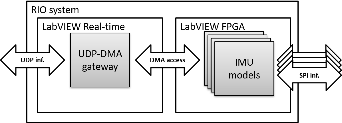
Figure 2. System overview
The hardware
A CompactRIO SOM from National Instruments was chosen as the processing device. It is a small, flexible, embedded computer for industrial applications that require high performance and reliability. It combines a dual core ARM processor running NI Linux Real-Time OS, a programmable Xilinx FPGA and a high-density connector to interface with the application-specific I/O of the Gateway.
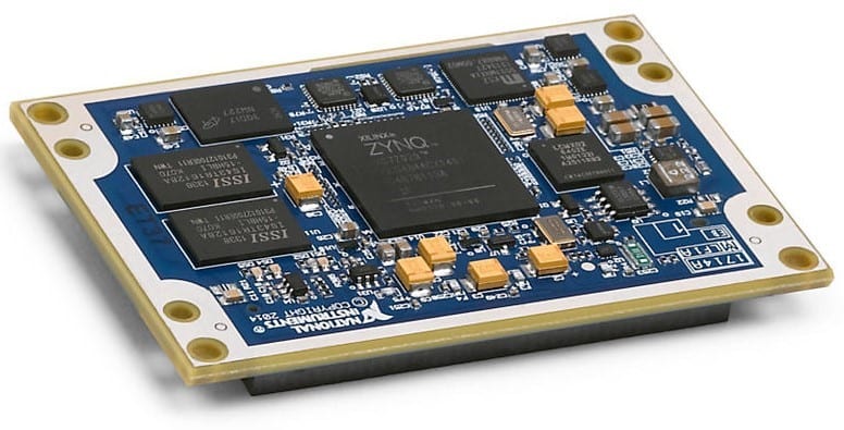
Figure 3. CompactRIO System on Module, sbRIO-9651 (SOM)
The SOM is mounted on a circuit board that has an RJ-45 connector for the Ethernet communication and circuitry to handle the SPI buses that are available through a DSUB connector. In this application, the SPI buses are working at 5V signal levels and due to the powerful FPGA, the buses can run at 10 MHz and above without problems. The circuit board, with the SOM, is mounted inside a rugged aluminum chassis that also has a fan for cooling of the device.
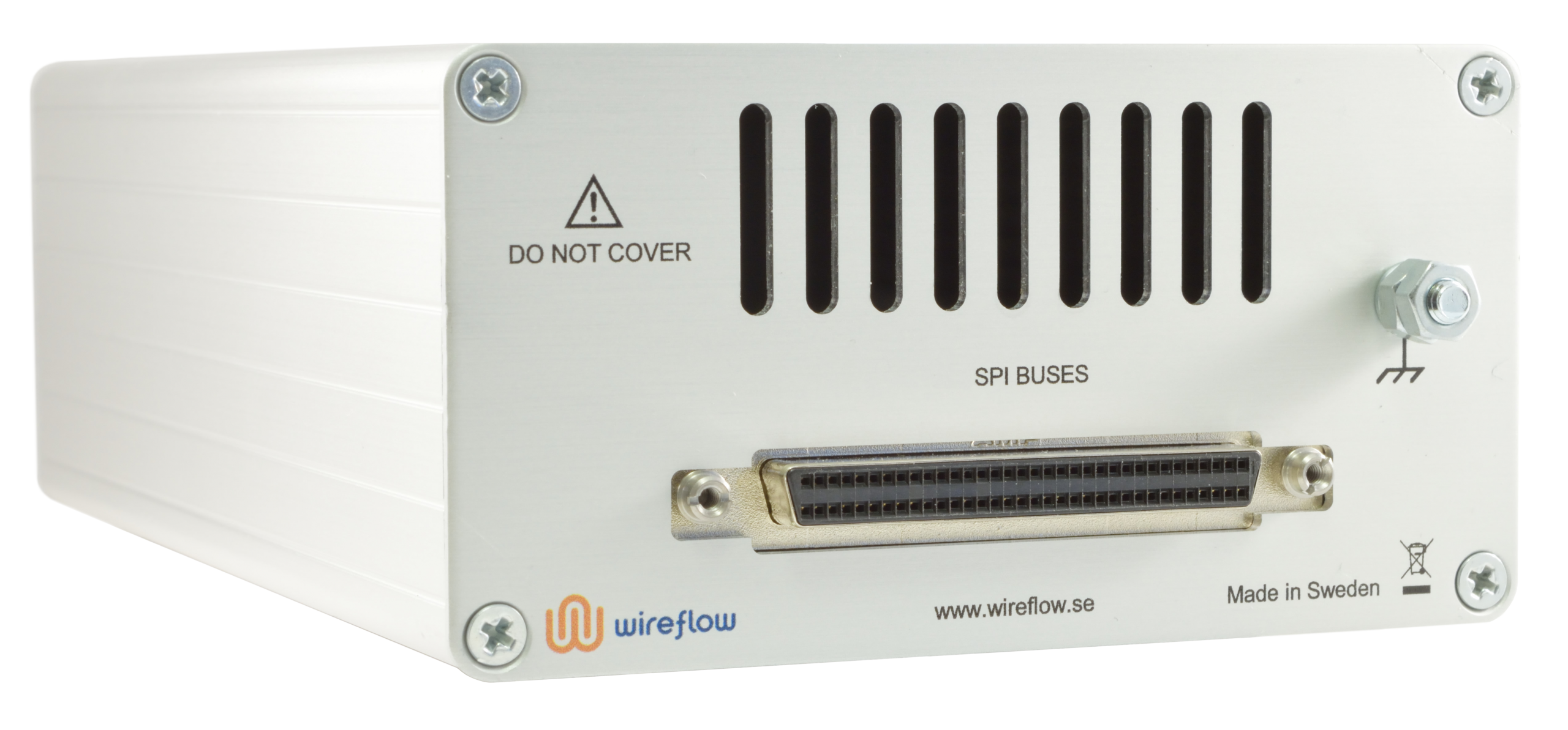
Figure 4. The UDP-SPI Gateway
The Gateway acts as slave on the SPI buses. Each such bus has four electrical wires. The three signals SCLK, MOSI and SS are received by the gateway and the MISO signal is transmitted from the Gateway to the ECU.
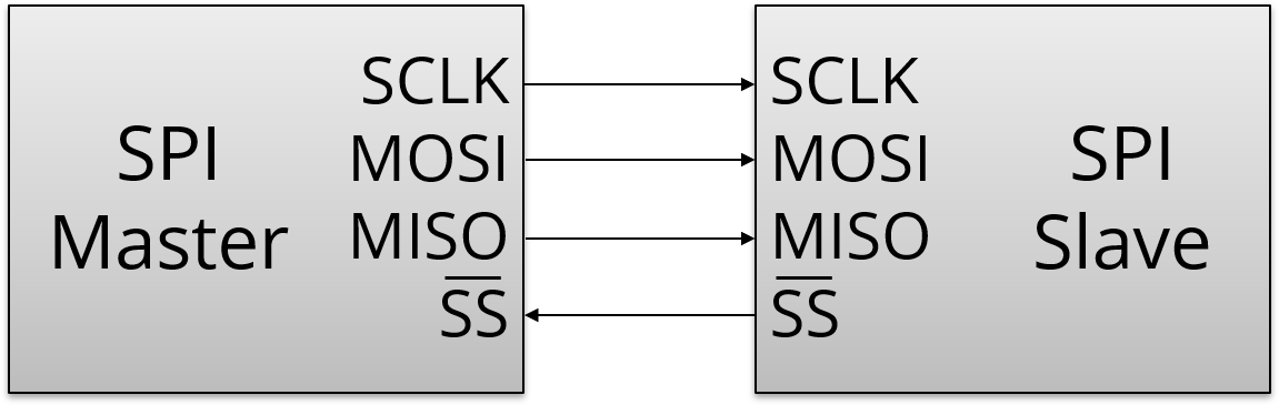
Figure 5. SPI point-to-point configuration
The Gateway can be configured to handle both positive and negative clock polarities (CPOL) and clock phases (CPHA).
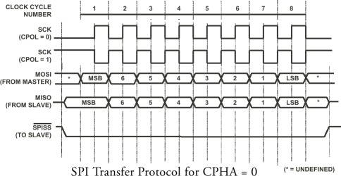
Figure 6. SPI timing diagram
The software
An external computer will stream simulated motion data to the Gateway over Ethernet as UDP packages. The motion data is written to the FPGA internal registers inside the Gateway.
The Gateway slave interfaces will respond individually on SPI read commands from the ECU with the sensor values being stored in the internal registers.
The LabVIEW FPGA software emulates the IMU sensors behavior in real time by responding to the SPI requests coming from the ECU. When the ECU is connected to the Gateway, the ECU believes it is connected to a number of real IMUs.
This setup makes it possible to perform verification of the ADAS functions implemented in the ECU in lab environment, instead of on the road.
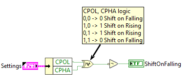
Figure 7. LabVIEW FPGA code that handles the Clock Polarity and Clock Phase